Research Article | | Peer-Reviewed

A High-Resolution Non-Volatile Floating Gate Transistor Memory Cell for On-Chip Learning in Analog Artificial Neural Networks

Received: 2 February 2025     Accepted: 17 February 2025     Published: 27 February 2025
Views:       Downloads:
Abstract

This paper proposes a high-resolution non-volatile memory cell design that addresses the most substantial limitations associated with the effective implementation of analog long-term memory storage solution. Prior research efforts often suffer from limited resolution, hindering their ability to accurately represent fine-grained weight adjustments required for effective learning in analog neuromorphic systems. This work effort has been channeled toward crafting conductive circuit designs using 90 nm complementary metal-oxide semiconductor technology for on-chip learning applications in analog neuromorphic systems. The operational mechanism of the cell involves the storage of charge on the floating gate of the NM0 transistor. The writing process is accomplished through hot-electron injection, while the erasure of stored information is executed via gate oxide tunneling. An advantageous feature of this cell is its capability to facilitate simultaneous reading and writing of data. The reduction of errors that may arise due to oxide mismatch or charge trapping is achieved through feedback control incorporation during the writing phase. The memory reveals clear synaptic behavior characteristics in storing and retrieving analog information reliably including, good memory cell resolution, good charge retention rate, reliable operation in noisy environments, and high resolution with faster learning with a power consumption of 1.06 µW and an output current of 10 µA under a typical operating voltage of 1 V. This strategic implementation enhances precise and reliable weight updates within neuromorphic analog artificial neural networks, which is essential for ensuring accurate on-chip learning outcomes as well as minimizing power consumption.

Published in Journal of Electrical and Electronic Engineering (Volume 13, Issue 1)
DOI 10.11648/j.jeee.20251301.17
Page(s) 82-91
Creative Commons

This is an Open Access article, distributed under the terms of the Creative Commons Attribution 4.0 International License (http://creativecommons.org/licenses/by/4.0/), which permits unrestricted use, distribution and reproduction in any medium or format, provided the original work is properly cited.

Copyright

Copyright © The Author(s), 2025. Published by Science Publishing Group

Keywords

Analog Artificial Neural Network, Floating Gate Memory, On-Chip Learning, Complementary Metal-Oxide Semiconductor

1. Introduction
Artificial Intelligence (AI) systems have driven significant advancements in the hardware and software domains. Analog Artificial Neural Networks (AANNs) have emerged as a promising tool for achieving energy-efficient and high-speed AI solutions. However, a major drawback to realizing AANNs is the lack of reliable on-chip learning analog memory cells for enabling real-time adaptation and dynamic behavior . For example, Zhang et al. proposed a capacitive storage memory structure with clock refresh to enable efficient accumulation . This structure suffers however from volatility and limited resolution. Also, Pechmann et al. introduced a multi-bit digital memory block that uses resistive cells for weight and bias storage in an embedded and distributed manner . This approach offers programming flexibility and reduced power consumption but exhibits low endurance. Moreover, integrating and directly into AANNs poses challenges due to mismatch issues and process variations. Furthermore, Huang et al. highlighted that current AI, primarily based on AANNs, faces two critical challenges: high energy consumption and limited ability to generalize knowledge and adapt to changes . These challenges open up new perspectives for implementing neuromorphic systems using analog devices. Floating Gate (FG) transistors exhibit an inherent aptitude for retaining non-volatile analog memory . Likewise, Haensch et al. indicated that material properties significantly influence AANN system-level characteristics, including speed, power, and classification accuracy . They reviewed the cross-bar-based computer in memory, considering both digital and analog memory while emphasizing co-design principles. Furthermore, Aguirre et al. investigated the use of memristors in neural network hardware , stipulating that memristors have potential low-resolution applications in medical informatics. On the same path, Chen et al. proposed a fully analog hyperbolic tangent function (tanh) implementation using phase-change memory . These analog-memory-based AANN architectures are compatible with on-chip learning neural networks, offering effective means for implementing neurons based on analog memory. Additionally, Won et al. explored a novel approach to multi-neuron connections using multi-terminal FG memristors . The study allows memory charging and discharging using horizontally distant multiple electrodes. Similarly, Winterfeld et al. proposed a MemFlash cell based on resistive switching . Unlike memristive devices, the MemFlash cell is purely an electronically based switching device with FG transistors as key elements, exhibiting memristive switching behavior. Also, Han et al. proposed a digital method utilizing an FG transistor-based in-memory computing chip . They achieve equivalent precision and high parallelism as Naqi et al. who developed an electronic synaptic device based on a synthesized memristor array , demonstrating memory performance, including retention and clear synaptic functions. Subsequently, Xu et al. unveiled a novel photonic activation function for neural networks that utilizes a non-volatile opto-resistive memory switch . This memory could have applications in analog networks, enabling flexible optical signal processing. Recent research has explored FG transistors for on-chip learning in AANNs, offering several advantages, including non-volatility, high density, and excellent programmability. Paliy et al. suggested a 180 nm Complementary Metal-Oxide Semiconductor (CMOS) single-poly technology platform based on analog vector-matrix multiplier architectures that use in-memory computation with FG multi-level non-volatility for analog neural network-integrated circuits , investigating accuracy through system simulations and temperature-dependent stored weights.
However, existing mentioned memory cells often suffer from limited resolution, hindering their ability to accurately represent fine-grained weight adjustments required for effective learning in AANNs. This work effort has been channeled toward crafting conductive circuit designs using 90 nm CMOS technology for on-chip learning AANNs, introducing an analog memory architecture using high-resolution non-volatile FG transistors to address the mentioned challenges. This memory offers several advantages for on-chip learning, including nonvolatile analog storage, high resolution, large dynamic range, on-chip simultaneous reading and writing operations, low power consumption with compact size, and compatibility with standard CMOS processing. By leveraging these advantages, this work aims to develop a memory cell capable of facilitating precise, persistent, and energy-efficient weight updates in AANNs. This design incorporates components such as an operational amplifier, which plays a pivotal role in the memory writing phase, transistors, and an adder circuit, which are integral to the weight modification synaptic process. This research contributes significantly to AANNs by paving the way for efficient and robust on-chip learning mechanisms, opening new avenues for developing intelligent systems in medical informatics.
The implemented memory in this work reveals clear synaptic behavior characteristics in storing and retrieving analog information reliably including, good memory cell resolution, good charge retention rate, reliable operation in noisy environments, and high resolution with faster learning with a power consumption of 1.06 µW and an output current of 10 µA under a typical operating voltage of 1 V. This strategic implementation enhances precise and reliable weight updates within neuromorphic analog artificial neural networks, which is essential for ensuring accurate on-chip learning outcomes as well as minimizing power consumption. This paper is organized as follows: the methodology used in designing the memory cell circuit block is presented in Section 2. Section 3 highlights the simulation results of the memory. Section 4 then focuses on the interpretation and validation of the obtained results. Finally, a brief conclusion and perspective for further studies are given in Section 5.
2. Materials and Methods
Although FG transistors are widely recognized as memory components , their application in silicon neural networks has been limited due to the lack of an effective bidirectional data-writing mechanism. Writing data involves moving charge carriers through the silicon dioxide-insulated gate of an FG transistor. Although Fowler–Nordheim tunneling and hot-electron injection are established techniques for this process, they have historical challenges. This work utilizes floating node connections of isolated n-type and p-type Metal–Oxide Semiconductor Field-Effect Transistor (MOSFET) tunneling to extract electrons from the FG by applying positive high voltages to a lightly doped n-type CMOS transistor (with an impurity concentration of approximately 1017/cm3) to create an environment where an n+ implant exists. Electrons are introduced into the FG through bidirectional tunneling. However, this method requires either dual polarity high voltages or a single polarity high voltage. Both options have drawbacks: dual polarity results in a low negative voltage compared to the substrate potential, while single polarity lacks simultaneous memory reading and writing support. Another approach is hot-electron injections in n-channel transistors requiring drain and gate voltages to exceed 3.1 V. This leads to high channel currents and power consumption unsuitable for on-chip learning in AANNs.
In contrast, rather than directly modifying a conventional n-type MOSFET channel, we enhance its injection rate through the introduction of a base implant by increasing PMOS substrate doping to reach Vtun of 6 V in an unprogrammed state, allowing sub-threshold channel currents at gate voltages sufficient to capture injected electrons. Selecting an injection transistor drain voltage of 5 V, ensures that the writing rate remains unaffected by minor variations in drain voltage, even though the drain breakdown voltage is approximately 7.25 V. The proposed analog memory cell in Figure 1 utilizes floating gate transistors and a comparator circuit coupled to an adder to achieve non-volatile weight storage and accurate weight updates without constant refresh. This paper assumes the following methodology for the erasing, writing, and reading processes: Firstly, the memory cell is reset to its initial state before writing a new weight value. A positive high-voltage, Vtun is applied to the control gate of the FG. This voltage induces Fowler-Nordheim tunneling, removing electrons from the FG. As electrons are removed, the output voltage, Vout approaches ground level. After erasure, the Vtun voltage is lowered, disabling the tunneling current and preserving the erased state. Secondly, in the memory writing phase, the target voltage obtained from weight adjustment in the adder circuit is set by applying the desired memory voltage, Vin to the non-inverting input of the comparator, A. The comparator is enabled, causing its output to adjust the drain voltage of the injection transistor, PM1 to a high level. The high drain voltage of PM1 generates a strong electric field, allowing electrons to be injected into the FG. As electrons are injected, the output voltage, Vout of the FG increases. When Vout surpasses the target voltage, Vin, the comparator changes its output state, lowering the drain voltage of PM1 to the ground. The comparator feedback ensures that Vout remains at the desired value Vin, as modeled by equation (1). Finally, the stored weight value is obtained by directly measuring the output voltage, Vout of the FG through a feedback capacitor Ci during the reading process. Importantly, the non-destructive read operation is ensured by the charge stored on the feedback capacitor which maintains unchanged the stored weight.
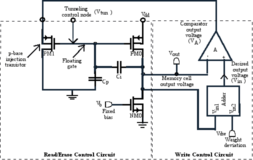
Figure 1. Analog memory cell circuit.
VA=0 if Vout<VinVin if VoutVin(1)
Furthermore, transistor NM0 depicted in Figure 1 is used for biasing. The amplifier formed by NM0 and PM0 drives the output node. Utilizing subthreshold channel currents allows for rail-to-rail output voltages and ultra-low power consumption. Transistor, PM1 facilitates hot-electron injection. The floating gate voltage must be maintained between 5V and 6V, requiring a supply voltage of 6-7 V to achieve reasonable injection rates. Capacitor Cp is the primary parasitic element, coupling from Ci to the ground for attenuating undesired signals. Additionally, this capacitor is intentionally used to fine-tune the frequency response of the memory. Additionally, during the memory writing phase, electron injection causes Vout to slew upwards, at a rate set approximately by equation (2). The term dVout/dt represents the output voltage rate of change, Vout over time, essentially how quickly the voltage increases during the writing process. Iinj, the injection current flows into the FG and causes the output voltage to rise. Ci represents the input capacitance, which measures how much charge the FG can store. This equation establishes a direct relationship between Iinj and the rate of change of Vout during the writing process. The rate at which the memory cell is written is adjusted by controlling the injection current Iinj.
dVoutdt=IinjCi(2)
Moreover, each weight in the AANN is represented by a specific voltage level stored in the analog memory. The weight update mechanism involves changing the voltage stored in the memory cell, reflecting the weight adjustments dictated by the backpropagation algorithm which calculates the amount of change needed for each weight based on the error signals and the learning rate. These updated weights correspond to the desired output voltages of the memory cell, obtained by adding the existing weight values, Vout, (corresponding to the actual output voltages of the memory cell) to the calculated weight deviation, ΔVdw as in equation (3).
Vout(t+1)=Vout(t)+ΔVdw(3)
The proposed analog memory cells underwent testing in controlled conditions. An external voltage source was employed for memory erasure, while an LM324 amplifier facilitated memory writing with the capacitance of feedback capacitor Ci chosen as 1 pF. This value represents a trade-off between speed and accuracy of the writing process. Optimal resolution on-chip learning applications under development utilize conventional lightly-doped drain high-voltage transistors presented in Table 1 to select memory cells for erasure. These transistors have high breakdown voltage, allowing them to handle high voltages required by the erasing process.
Table 1. Transistor dimensions for the memory block.

Transistor

Type

With (ƞm)

Length (µm)

NM0

NMOS

120

1.16

PM0

PMOS

120

0.465

PM1

PMOS

120

0.465

3. Results
3.1. Voltage Characterization
This section presents the comprehensive characterization results of the analog FG transistor memory cell output voltage behavior as depicted in Figure 2 to Figure 5. We systematically investigated the memory cell's response to variations in weight deviation voltage, focusing on key performance metrics including programmability, resolution, retention characteristics, and noise immunity.
First, the analog cell memory's voltages are depicted in Figure 2, revealing how the desired memory voltage, Vin, the comparator output voltage, VA, and memory output voltage, Vout, respond to changes in the weight deviation, Vdw. Vin, VA, and Vout are represented in black, green, and blue, respectively. The output voltage shows a desirable linear relationship with the weight deviation as required for accurate analog weight representation. A unity voltage gain is obtained between Vout and Vin for positive weight deviations, while the gain is approximately 0.96 for negative weight deviations. Thus, indicating significant memory cell sensitivity to weight updates.
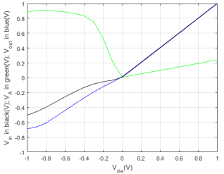
Figure 2. Voltage responses (Vin in black, VA in green, and Vout in blue) versus weight deviations.
Secondly, a scatter plot with Qinj on the x-axis and Vout on the y-axis is depicted in Figure 3, showing a linear relationship between injected charge and output voltage. This linear relationship with the slope steepness of 98.8 (close to the ideal value of 100) indicates good memory cell programmability. Furthermore, the small spacing between points on the line suggests good memory cell resolution with some slide degree of noise, allowing precise weight adjustments.
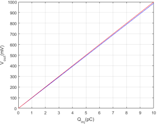
Figure 3. Programmability and resolution characteristics.
Thirdly, Figure 4 shows a line plot with Time on the x-axis and Vout on the y-axis, demonstrating how the output voltage decays over time after an initial charge is injected. The slope of -0.0005 (close to the ideal value of 0) with a relatively slow decay in Vout over time indicates a good charge retention rate. The charge-long retention time proves that long-term storage is desirable for AANNs.
Figure 4. Retention characteristics.
Finally, Figure 5 depicts a plot displaying the output voltage as a function of the noise amplitude applied to the memory cell. This plot shows an approximately 10 % increase in Vout as noise amplitude increases, with a maximum noise amplitude tolerance of 100 mV. The noise amplitude is within the tolerance range of the memory cell, indicating reliable operation in noisy environments.
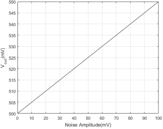
Figure 5. Noise immunity characteristics.
3.2. Memory Performance
This section delves into the memory cell's comprehensive performance analysis, exploring its injection efficiency, reading characteristics, memory accuracy, and writing error rate, as depicted in Figure 6 to Figure 9. This multifaceted analysis provides insights into the cell's abilities for storing and retrieving analog information, paving the way for its future integration into complex neuromorphic systems.
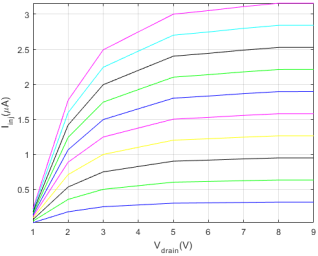
Figure 6. Injection efficiency.
The injection efficiency is depicted in Figure 6, illustrating multiple curve plots of Iinj versus Vdrain for different Vgate values. Each curve shows a roughly exponential increase in Iinj as Vdrain increases with some degree of linearity before the saturation regime indicating good injection. As Vgate increases, the curves shift upward with steeper slopes, implying higher gate voltages lead to higher injection currents at the same drain voltage. This plot demonstrates the impact of the gate voltage on the device's injection efficiency.
Furthermore, the reading characteristic of the analog cell memory is depicted in Figure 7, illustrating multiple curve plots Idrain over time for different Vdw values. This plot shows a slight increase in Idrain with increasing Vdw, demonstrating the analog memory cell takes a maximum of 1 s to memorize the written voltage. This is a crucial feature for understanding device behavior within an AANN.
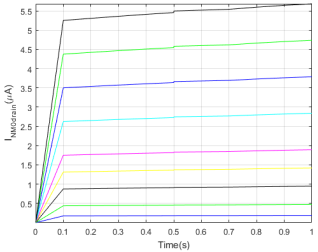
Figure 7. Reading characteristics.
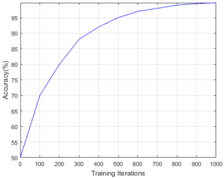
Figure 8. Memory accuracy performance.
Moreover, Figure 8 depicts the memory performance while Figure 9 shows the memory writing error, with both illustrations trained over 1000 iterations using the Wisconsin dataset. Incorporating this cell in a 9-10-2 AANN architecture for breast cancer diagnosis attains a memory erasing/reading accuracy of 99.8 % with 0.2 % writing error, indicating a high resolution with faster learning.
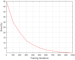
Figure 9. Memory writing error.
3.3. Memory Effectiveness
This section analyzes the cell effectiveness through the hysteresis loop characteristic and the total power consumption during operation, as depicted in Figure 10 to Figure 11. It recognizes the importance of energy efficiency for AANNs. Examining its effectiveness achieves a comprehensive understanding of the trade-offs and integration of this cell into energy-constrained neuromorphic systems.
The hysteresis characteristic of the memory cell is depicted in Figure 10. The drain current increases as Vds increase from negative to positive in sweep-up, indicating that the memory is in its programming state. On the other hand, the drain current decreases as Vds decrease from positive to negative, indicating that the memory is in its erasing state. It is observed that the sweep-up and sweep-down curves do not overlap, indicating hysteresis and forming a closed loop S-shaped with transistors operating in the subthreshold regime. The hysteresis loop indicates the memory's ability to retain its previous state to some extent after a voltage change. The hysteresis loop width, ΔV, indicates the memory can retain up to 2 V which is more than enough for AANN applications.
The memory cell's total power consumption is depicted in Figure 11. It is known that the total power consumption of a circuit is obtained by calculating the area under its graph. Thus, the memory cell’s power consumption is 1.06 µW under a typical operating voltage of 1 V. This power value is low compared to similar analog memory technologies.
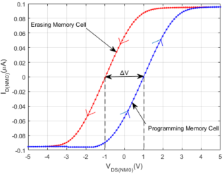
Figure 10. Hysteresis sweep.
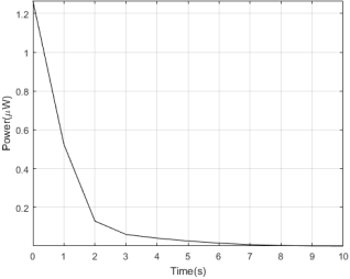
Figure 11. Total power.
4. Discussion
The results presented in the previous section reveal promising performance characteristics in storing and retrieving analog information reliably, providing a detailed understanding of the cell's operational characteristics and serving as a foundation for evaluating its suitability for applications in analog neural networks and other analog signal processing tasks. Moreover, this indicates that the injection rate remains nearly constant across a broad range of drain voltages. This phenomenon results from two opposing processes. Firstly, when the drain voltage exceeds the gate voltage, the electric field within the oxide layer hinders electron movement toward the gate, causing the injected electrons to return to the drain. Consequently, the injection efficiency diminishes as the drain voltage increases. Secondly, a rise in drain voltage enhances the electric field in the drain-to-channel depletion layer, significantly boosting the number of electrons with enough energy to overcome the 3.0 eV oxide potential barrier. Over a wide range of drain voltages, the reduction in efficiency is almost perfectly balanced by the growing number of hot electrons, resulting in a nearly constant injection rate. By setting the injection transistor drain voltage to 5 V for memory writing, the writing rate becomes stable despite minor variations in drain voltage.
Furthermore, the offset error could be influenced by the loop’s time constant . This offset primarily arises because the error signal in the negative feedback loop is the injection current, which is determined by the drain voltage of the injection transistor. However, the injection transistor's drain-to-gate capacitance, Cdg, creates an alternative positive feedback loop. This feedback loop introduces hysteretic responses, aiding the comparator in fully switching once it starts slewing in an unavoidable offset error at the cell output. Moreover, maintaining the memory cell precision relies heavily on power supply rejection . The FG is referenced to the positive supply Vdd through transistor PM0, making the cell suitable for driving loads that are also referenced to Vdd. Ideally, the cell’s output follows variations in Vdd with unity gain. The design parameters needed to achieve this unity gain from Vdd to Vout is obtained as follows:
First, by examining the feedback loop created by Ci, NM0, and PM0, with Vdd serving as the input and Vout as the output. Given an infinite loop gain, the resulting closed-loop transfer function is governed by equation (4).
G=VoutVddT==Ci+CpCi=1+CpCi(4)
Secondly, we wish to obtain a unity gain closed-loop transfer function from Vdd to Vout. This can be accomplished by setting a finite loop gain, T to offset α. The resulting closed-loop transfer function is given by equation (5).
VoutVdd=GT1+T=G1+1T=1+α1+1T(5)
Choosing α=CpCi=1T gives VoutVdd=1
The clear hysteresis loop observed in the I-V curves demonstrates the key memory effect of this device. The width of the loop suggests that the cell can reliably store analog values for a significant period, which is crucial for memory functionality. The results on programmability and resolution suggest that the cell can be precisely controlled to store a range of analog values. The good linear relationship between the injected charge and output voltage indicates effective programmability with resolution permitting the fine-tuning of the stored values. The retention characteristics demonstrate the memory cell's ability to maintain stored analog information over time with an encouraging observed decay rate. While noise tolerance and writing error are expected, the observed sensitivity suggests that the cell is within reliable tolerance operation in noisy environments with minute error, indicating that slide optimization is needed. The observed total power consumption suggests that the device could be integrated into low-power systems.
Additionally, the results demonstrate that the analog FG transistor memory cell possesses promising characteristics for analog information storage and processing. This memory cell could be potentially integrated into more complex networks, for example, , for advanced analog signal processing in neuromorphic computing applications.
5. Conclusions
This work presented the design and characterization of a high-resolution non-volatile FG transistor memory cell suitable for on-chip learning in AANNs. The proposed cell utilizes a novel combination of advanced techniques, including hot-electron injection by introducing base implants and gate oxide tunneling to achieve high-density, non-volatile storage with exceptional analog characteristics. The results demonstrate the feasibility of the proposed cell as an efficient component for on-chip learning. The high-resolution analog storage capacity, low power consumption, and non-volatility of the cell offer significant advantages over conventional digital memory approaches, paving the way for efficient and scalable analog neuromorphic systems. The demonstrated memory characteristics offer the potential for implementing highly accurate analog synaptic weights within the AANNs, thereby enabling efficient and precise learning. The study highlights the significant potential of FG memory cells for enabling truly integrated, low-power, and high-performance on-chip learning systems. Future research will focus on further optimization of the cell design and integration into larger-scale AANN architectures for real-world applications. This work paves the way for developing sophisticated neuromorphic systems that mimic the human brain's computational capabilities and revolutionize artificial intelligence and machine learning research.
Abbreviations

AI

Artificial Intelligence

AANNs

Analog Artificial Neural Networks

FG

Floating Gate

CMOS

Complementary Metal-Oxide Semiconductor

MOSFET

Metal–Oxide Semiconductor Field-Effect Transistor

Author Contributions
Koagne Longpa Tamo Silas: Conceptualization, Investigation, Methodology, and Writing – original draft
Djimeli-Tsajio Alain Bernard: Supervision, Writing –review & editing
Fotsing Talla Bernard: Formal Analysis
Lienou Jean-Pierre: Visualization
Geh Wilson Ejuh: Project administration and Writing – review & editing
Funding
No funding is raised for this research.
Data Availability Statement
Not applicable.
Conflicts of Interest
The authors declare no conflicts of interest.
References
[1] Kumar, A., Beeraka, S. M., Singh, J., Gupta, B. An On-Chip Trainable and Scalable In-Memory ANN Architecture for AI/ML Applications. Circuits, Systems, and Signal Processing. 2023, 42(5), 2828-2851.
[2] Zhang, B., Saikia, J., Meng, J., Wang, D., Kwon, S., Myung, S., Seok, M. MACC-SRAM: A Multistep Accumulation Capacitor-Coupling In-Memory Computing SRAM Macro for Deep Convolutional Neural Networks. IEEE Journal of Solid-State Circuits. 2023.
[3] Pechmann, S., Mai, T., Potschka, J., Reiser, D., Reichel, P., Breiling, M., Hagelauer, A. A low-power RRAM memory block for embedded, multi-level weight and bias storage in artificial neural networks. Micromachines. 2021, 12(11), 1277.
[4] Castriotta, M., Prati, E., Ferrari, G. Cryogenic characterization and modeling of a CMOS floating-gate device for quantum control hardware. Solid-State Electronics. 2022, 189, 108190.
[5] Huang, Y., Kiani, F., Ye, F., Xia, Q. From memristive devices to neuromorphic systems. Applied Physics Letters. 2023, 122(11).
[6] Haensch, W., Raghunathan, A., Roy, K., Chakrabarti, B., Phatak, C. M., Wang, C., Guha, S. Compute in‐memory with non‐volatile elements for neural networks: A review from a co‐design perspective. Advanced Materials. 2023, 35(37), 2204944.
[7] Aguirre, F., Sebastian, A., Le Gallo, M., Song, W., Wang, T., Yang, J. J., Lanza, M. Hardware implementation of memristor-based artificial neural networks. Nature communications. 2024, 15(1), 1974.
[8] Chen, Z., Li, X., Zhu, X., Liu, H., Tong, H., Miao, X. Full-analog implementation of activation function based on phase-change memory for artificial neural networks. IEEE Transactions on Industrial Electronics. 2023.
[9] Won, U. Y., Vu, A., Q., Park, S. B., Park, M. H., Dam Do, V., Park, H. J., Yu, W. J. (2023). Multi-neuron connection using multi-terminal floating–gate memristor for unsupervised learning. Nature Communications. 2023, 14(1), 3070.
[10] Winterfeld, H., Kohlstedt, H., Ziegler, M. MemFlash—Floating Gate Transistors as Memristors. In Bio-Inspired Information Pathways: From Neuroscience to Neurotronics. 2023, 115-128.
[11] Han, R., Huang, P., Xiang, Y., Hu, H., Lin, S., Dong, P., Kang, J. Floating Gate Transistor‐Based Accurate Digital In‐Memory Computing for Deep Neural Networks. Advanced Intelligent Systems, 2022, 4(12), 2200127.
[12] Naqi, M., Kang, M. S., Liu, N., Kim, T., Baek, S., Bala, A., Kim, S. Multilevel artificial electronic synaptic device of direct grown robust MoS2 based memristor array for in-memory deep neural network. npj 2D. Materials and Applications. 2022, 6(1), 53.
[13] Xu, Z., Tang, B., Zhang, X., Leong, J. F., Pan, J., Hooda, S., Thean, A. V. Y. Reconfigurable nonlinear photonic activation function for photonic neural network based on non-volatile opto-resistive RAM switch. Light: Science & Applications, 2022, 11(1), 288.
[14] Paliy, M., Rizzo, T., Ruiu, P., Strangio, S., Iannaccone, G. Single-poly floating-gate memory cell options for analog neural networks. Solid-State Electronics. 2021, 185, 108062.
[15] Jeong, H., Woo, S., Choi, J., Cho, H., Kim, Y., Kong, J. T., Kim, S. Fast and expandable ANN-based compact model and parameter extraction for emerging transistors. IEEE Journal of the Electron Devices Society. 2023, 11, 153-160.
[16] Chen, H., Xu, Z., Xiong, W., Zhang, J., Xu, X., Wang, H., Kong, W. Fabrication and optimization of aggressively scaled Dual-Bit/Cell Split-Gate Floating-Gate flash memory cell in 55-nm node technology. Solid-State Electronics. 2022, 194, 108316.
[17] Mehta, D., Rahman, M., Aono, K., Chakrabartty, S. An adaptive synaptic array using Fowler–Nordheim dynamic analog memory. Nature communications. 2022, 13(1), 1670.
[18] Sonnadara, C., Shah, S. On-Chip Adaptation for Reducing Mismatch in Analog Non-Volatile Device Based Neural Networks. In 2024 IEEE International Symposium on Circuits and Systems (ISCAS). 2024, 1-5, IEEE.
[19] Huang, H. M., Wang, Z., Wang, T., Xiao, Y., Guo, X. Artificial neural networks based on memristive devices: From device to system. Advanced Intelligent Systems. 2020, 2(12), 2000149.
[20] Gan, L., Wang, C., Chen, L., Zhu, H., Sun, Q., Zhang, D. W. An Enhanced Floating Gate Memory for the Online Training of Analog Neural Networks. IEEE Journal of the Electron Devices Society. 2020, 8, 84-91.
[21] Djimeli-Tsajio A. B., Silas, K. L. T., Jean-Pierre, L. T., Thierry, N., Ejuh, G. W. (2024). Breast Cancer Diagnosis with Machine Learning Using Feed-Forward Multilayer Perceptron Analog Artificial Neural Network. International Journal of Electrical and Electronic Engineering & Telecommunications. 2024, 13(6), 427-441.
Cite This Article
  • APA Style

    Silas, K. L. T., Bernard, D. A., Bernard, F. T., Jean-Pierre, L., Ejuh, G. W. (2025). A High-Resolution Non-Volatile Floating Gate Transistor Memory Cell for On-Chip Learning in Analog Artificial Neural Networks. Journal of Electrical and Electronic Engineering, 13(1), 82-91. https://doi.org/10.11648/j.jeee.20251301.17

    Copy | Download

    ACS Style

    Silas, K. L. T.; Bernard, D. A.; Bernard, F. T.; Jean-Pierre, L.; Ejuh, G. W. A High-Resolution Non-Volatile Floating Gate Transistor Memory Cell for On-Chip Learning in Analog Artificial Neural Networks. J. Electr. Electron. Eng. 2025, 13(1), 82-91. doi: 10.11648/j.jeee.20251301.17

    Copy | Download

    AMA Style

    Silas KLT, Bernard DA, Bernard FT, Jean-Pierre L, Ejuh GW. A High-Resolution Non-Volatile Floating Gate Transistor Memory Cell for On-Chip Learning in Analog Artificial Neural Networks. J Electr Electron Eng. 2025;13(1):82-91. doi: 10.11648/j.jeee.20251301.17

    Copy | Download

  • @article{10.11648/j.jeee.20251301.17,
      author = {Koagne Longpa Tamo Silas and Djimeli-Tsajio Alain Bernard and Fotsing Talla Bernard and Lienou Jean-Pierre and Geh Wilson Ejuh},
      title = {A High-Resolution Non-Volatile Floating Gate Transistor Memory Cell for On-Chip Learning in Analog Artificial Neural Networks
    },
      journal = {Journal of Electrical and Electronic Engineering},
      volume = {13},
      number = {1},
      pages = {82-91},
      doi = {10.11648/j.jeee.20251301.17},
      url = {https://doi.org/10.11648/j.jeee.20251301.17},
      eprint = {https://article.sciencepublishinggroup.com/pdf/10.11648.j.jeee.20251301.17},
      abstract = {This paper proposes a high-resolution non-volatile memory cell design that addresses the most substantial limitations associated with the effective implementation of analog long-term memory storage solution. Prior research efforts often suffer from limited resolution, hindering their ability to accurately represent fine-grained weight adjustments required for effective learning in analog neuromorphic systems. This work effort has been channeled toward crafting conductive circuit designs using 90 nm complementary metal-oxide semiconductor technology for on-chip learning applications in analog neuromorphic systems. The operational mechanism of the cell involves the storage of charge on the floating gate of the NM0 transistor. The writing process is accomplished through hot-electron injection, while the erasure of stored information is executed via gate oxide tunneling. An advantageous feature of this cell is its capability to facilitate simultaneous reading and writing of data. The reduction of errors that may arise due to oxide mismatch or charge trapping is achieved through feedback control incorporation during the writing phase. The memory reveals clear synaptic behavior characteristics in storing and retrieving analog information reliably including, good memory cell resolution, good charge retention rate, reliable operation in noisy environments, and high resolution with faster learning with a power consumption of 1.06 µW and an output current of 10 µA under a typical operating voltage of 1 V. This strategic implementation enhances precise and reliable weight updates within neuromorphic analog artificial neural networks, which is essential for ensuring accurate on-chip learning outcomes as well as minimizing power consumption.
    },
     year = {2025}
    }
    

    Copy | Download

  • TY  - JOUR
    T1  - A High-Resolution Non-Volatile Floating Gate Transistor Memory Cell for On-Chip Learning in Analog Artificial Neural Networks
    
    AU  - Koagne Longpa Tamo Silas
    AU  - Djimeli-Tsajio Alain Bernard
    AU  - Fotsing Talla Bernard
    AU  - Lienou Jean-Pierre
    AU  - Geh Wilson Ejuh
    Y1  - 2025/02/27
    PY  - 2025
    N1  - https://doi.org/10.11648/j.jeee.20251301.17
    DO  - 10.11648/j.jeee.20251301.17
    T2  - Journal of Electrical and Electronic Engineering
    JF  - Journal of Electrical and Electronic Engineering
    JO  - Journal of Electrical and Electronic Engineering
    SP  - 82
    EP  - 91
    PB  - Science Publishing Group
    SN  - 2329-1605
    UR  - https://doi.org/10.11648/j.jeee.20251301.17
    AB  - This paper proposes a high-resolution non-volatile memory cell design that addresses the most substantial limitations associated with the effective implementation of analog long-term memory storage solution. Prior research efforts often suffer from limited resolution, hindering their ability to accurately represent fine-grained weight adjustments required for effective learning in analog neuromorphic systems. This work effort has been channeled toward crafting conductive circuit designs using 90 nm complementary metal-oxide semiconductor technology for on-chip learning applications in analog neuromorphic systems. The operational mechanism of the cell involves the storage of charge on the floating gate of the NM0 transistor. The writing process is accomplished through hot-electron injection, while the erasure of stored information is executed via gate oxide tunneling. An advantageous feature of this cell is its capability to facilitate simultaneous reading and writing of data. The reduction of errors that may arise due to oxide mismatch or charge trapping is achieved through feedback control incorporation during the writing phase. The memory reveals clear synaptic behavior characteristics in storing and retrieving analog information reliably including, good memory cell resolution, good charge retention rate, reliable operation in noisy environments, and high resolution with faster learning with a power consumption of 1.06 µW and an output current of 10 µA under a typical operating voltage of 1 V. This strategic implementation enhances precise and reliable weight updates within neuromorphic analog artificial neural networks, which is essential for ensuring accurate on-chip learning outcomes as well as minimizing power consumption.
    
    VL  - 13
    IS  - 1
    ER  - 

    Copy | Download

Author Information
  • Research Unit of Automation and Applied Computer Science URAIA, University of Dschang, Bandjoun, Cameroon

    Biography: Koagne Longpa Tamo Silas earned his Technical School Teacher’s Training Diploma I (DIPET I) in Electrical and Electronics Engineering, option Electronics at the University of Bamenda in 2018. His commitment to academic excellence led him to obtain a Technical School Teacher’s Training Diploma II (DIPET II) in Electrical and Electronics Engineering, option Electronics at the University of Bamenda in 2020. His passion for research in Electrical and Electronics Engineering motivated him to further his studies at the University of Dschang where he obtained a Bachelor's Degree in Sciences and Technology (BSc) in Physics, option Electrical, Electronics, and Automation (EEA) in 2021 and followed by a Master Degree of Sciences and Technology (MSc) in Physics option Electrical, Electronics and Automation (EEA) in 2022. He currently stands at the forefront of technology and scientific research as a UR.A.I.A. member and Ph.D. Student in Physics specializing in Electronics at the University of Dschang.

    Research Fields: Medical informatics, Artificial Intelligence, Electrical and Electronic Engineering, Analog Artificial Neural Networks, Embedded Systems

  • Research Unit of Automation and Applied Computer Science URAIA, University of Dschang, Bandjoun, Cameroon; Department of Telecommunication and Network Engineering, IUT-FV-University of Dschang, Bandjoun, Cameroon

    Biography: Djimeli Tsajio Alain Bernard received a B.S. (2001) and M.S. with thesis (2004) from the Faculty of Science of the University of Yaoundé I and a Ph.D. (2016) from the Faculty of Science of the University of Dschang, all in Cameroon in the field of Physics option Electronics. Since 2006, he has joined Fotso Victor University Institute of Technology of the University of Dschang as a lecturer in the Department of Telecommunication and Network Engineering. He is a member of UR.A.I.A. of the present university where he is carrying out research in the field of Artificial Intelligence for biomedical process. He is the author of more than 10 research papers.

    Research Fields: Telecommunications Engineering, Computer and Network Engineering, Artificial Intelligence, Biomedical Informatics, Software Engineering

  • Research Unit of Automation and Applied Computer Science URAIA, University of Dschang, Bandjoun, Cameroon; Department of Computer Engineering, IUT-FV-University of Dschang, Bandjoun, Cameroon

    Biography: Fotsing Talla Bernard is a researcher at the University of Dschang in Cameroon. His research interests include Information Systems (Business Informatics), Software Engineering, and Programming Languages. He joined Fotso Victor University Institute of Technology of the University of Dschang as a lecturer in the Department of Computer Engineering. He is a member of UR.A.I.A. of the present university where he conducts research. He is the author of 6 research papers.

    Research Fields: Information Systems, Business Informatics, Software Engineering, Programming Languages, Computer Engineering

  • Research Unit of Automation and Applied Computer Science URAIA, University of Dschang, Bandjoun, Cameroon; Department of Computer Engineering, IUT-FV-University of Dschang, Bandjoun, Cameroon

    Biography: Lienou Jean-Pierre obtained his MSc in Systems and Networks at Kyiv Polytechnic Institute of the National Technical University of Ukraine in 1994. He obtained a Ph.D. in 2015 at Yaoundé National Advanced School of Engineers of the University of Yaoundé I, Cameroon. He is now an Associate Professor of Computer Science and was posted as Head of the Department of Computer Engineering in the College of Technology at the University of Bamenda in 2017. He is a member of the International Association of Engineers. He received the first Cameroon National Prize of Innovation in Embedded Systems and is currently a peer reviewer in few International Journal of Computer Science.

    Research Fields: Telecommunications Engineering, Computer Engineering, Software Engineering, Computer Communications (Networks), Artificial Intelligence

  • Department of General and Scientific Studies, IUT-FV-University of Dschang, Bandjoun, Cameroon; Department of Electrical and Electronic Engineering, NAHPI-University of Bamenda, Bambili, Cameroon

    Biography: Geh Wilson Ejuh is a distinguished academic researcher in Electrical and Electronic Engineering. He earned a BSc in Physics-Chemistry in 2003, obtaining an MSc in Physics in 2006. In 2013, he obtained his Ph.D. in Physics option Materials Sciences from the Faculty of Science of the University of Yaoundé 1, Cameroon. In 2014, he was promoted to Lecturer, in 2019 to Associate Professor, and in 2023, he was promoted to Professor of Physics. He was posted as Head of Services for Teaching and Academic Activities in NAHPI in 2017 and 2021 as Head of Services for continuous training in NAHPI, University of Bamenda. Currently, he contributes his expertise at the University of Dschang, IUT-FV Bandjoun, Cameroon, within the General and Scientific Studies department, and at the National Higher Polytechnic Institute of the University of Bamenda, in the Department of Electrical and Electronic Engineering.

    Research Fields: Electrical and Electronics Engineering, Optoelectronics, Photonic, Thermodynamics Properties, Organic and Pharmaceutical molecules