This research evaluates the switching performance of silicon carbide (SiC) transistors compared to silicon (Si) transistors through a double pulse test. The performance was analyzed by measuring switching losses, di/dt, overshooting and switching times. The results demonstrated that switching losses, as well as rise and fall times, are reduced by half in SiC transistors. However, some overshoot in voltage and current waveforms was observed due to the high switching speed of SiC transistors. Subsequently, the impact of parasitic capacitive and inductive elements on the switching performance and switching losses in SiC transistors was studied across various values. The findings revealed that these parasitic components significantly affect the current balancing among SiC transistors in parallel driving circuits, with a recorded current difference of up to 6 A between transistors due to variations in internal capacitor values and the inductive effects resulting from current changes over time in the transistor's terminal paths. Simulation was conducted using LTspice software. In conclusion, the research results were summarized, and conclusions regarding the impact of internal elements on transistor performance were presented.
| Published in | Journal of Electrical and Electronic Engineering (Volume 13, Issue 4) |
| DOI | 10.11648/j.jeee.20251304.14 |
| Page(s) | 184-204 |
| Creative Commons |
This is an Open Access article, distributed under the terms of the Creative Commons Attribution 4.0 International License (http://creativecommons.org/licenses/by/4.0/), which permits unrestricted use, distribution and reproduction in any medium or format, provided the original work is properly cited. |
| Copyright |
Copyright © The Author(s), 2025. Published by Science Publishing Group |
Switching Losses, Static Current, Dynamic Current, Double Pulse Testing, Parasitic Inductance, Parasitic Capacitance, Current Balancing, Parallel SiC MOSFET
Dc Bus Voltage | 400 volts |
Decoupling Capacitor | 220µF |
Load | 1mH-inductive |
Transistor Type | R6020PNJ, (Si) |
C3M0045065K, (SiC) | |
Positive driving voltage | +15 volt |
Negative driving voltage | -5 volt |
Drain-Source On-State Resistance | 190mΩ (Si MOSFET) |
45mΩ (SiC MOSFET) | |
Total Time of two pulses | 70 µsec |
Gate Resistor | 10Ω |
Parameter | (μJ) | (ns) |
|---|---|---|
Si Mosfet | 70.71 | 60 |
SiC Mosfet | 41.75 | 24 |
Parameter | (μJ) | (ns) |
|---|---|---|
Si Mosfet | 82.99 | 74 |
SiC Mosfet | 40.77 | 40 |
Dc Bus voltage | 400 volts |
|---|---|
Decoupling Capacitor | 1000µF |
Load | 1mH |
Transistor Type | C3M0045065K, (SiC) |
Positive driving voltage | +15 volt |
Negative driving voltage | -5 volt |
Drain-Source On-State Resistance | 45mΩ |
Ciss (input Capacitance) | 1621pf |
Crss (Reverse Capacitance) | 8pf |
Coss (output Capacitance) | 101pf |
Rg | [1, 5, 10, 15, 20] Ω |
Inductive effect of di/dt through the drain. | [1, 10, 30, 50, 70] nH |
Inductive effect of di/dt through the source. | [1, 3, 6, 9, 12] nH |
Inductive effect of di/dt through the gate. | [1, 5, 10, 15, 20] nH |
Drain to Source Capacitance. | [75.9, 110, 125] pf |
Gate to Drain Capacitance. | [6, 8, 10, 15, 20] pf |
Gate to Source Capacitance. | [1.5, 2.5, 3.5, 4.5, 5.5] nF |
Rg (Ω) | (μJ) | (μJ) | (ns) | (ns) |
|---|---|---|---|---|
5 | 45.36 | 63.25 | 86.52 | 25.29 |
10 | 76.77 | 82.04 | 80.9 | 34.7 |
15 | 110.57 | 90.06 | 100.34 | 44.46 |
20 | 143.63 | 118.1 | 114.21 | 59.89 |
Ls (nH) | (μJ) | (μJ) | (ns) | (ns) |
|---|---|---|---|---|
1 | 70.72 | 80.32 | 38.07 | 36.58 |
3 | 81.66 | 84.57 | 44.74 | 40.79 |
6 | 84.16 | 88.28 | 52.41 | 40.79 |
9 | 88.74 | 93.32 | 59.33 | 35.55 |
12 | 91.05 | 103.17 | 61.55 | 37.55 |
Ld (nH) | (μJ) | (μJ) | (ns) | (ns) |
|---|---|---|---|---|
1 | 82.15 | 85.48 | 40.43 | 33.62 |
10 | 84.82 | 88.57 | 43.3 | 34.11 |
30 | 93.82 | 94.09 | 43.9 | 34.61 |
50 | 101.69 | 106.93 | 48.05 | 41.53 |
70 | 115.98 | 118.34 | 48.65 | 46.22 |
Cgs (nf) | (μJ) | (μJ) | (ns) | (ns) |
|---|---|---|---|---|
1.5 | 75.61 | 80.17 | 50.72 | 33.44 |
2.5 | 80.81 | 90.17 | 58.4 | 38.34 |
3.5 | 87.63 | 99.41 | 64.74 | 44.46 |
4.5 | 96.9 | 109.2 | 76.42 | 47.3 |
5.5 | 104.48 | 118.76 | 88.11 | 52.21 |
Cgd (pf) | (μJ) | (μJ) | (ns) | (ns) |
|---|---|---|---|---|
6 | 77.15 | 82.15 | 33.62 | 33.22 |
8 | 84.23 | 88.35 | 37.28 | 33.91 |
10 | 85.76 | 90.87 | 37.82 | 34.61 |
15 | 91.48 | 93.35 | 42.27 | 41.18 |
20 | 93.64 | 94.43 | 43.26 | 41.2 |
Cds (pf) | (μJ) | (μJ) | (ns) | (ns) |
|---|---|---|---|---|
75 | 77.35 | 79 | 42.54 | 33.6 |
90 | 79.35 | 80.79 | 43.99 | 33.89 |
110 | 83.56 | 85.36 | 45.79 | 38.65 |
125 | 89.71 | 93.93 | 46.33 | 40.81 |
Dc Bus voltage | 400 volts |
|---|---|
Decoupling Capacitor | 1000µF |
Load | 100uH |
Transistor Type | C3M0045065K, (SiC) |
Positive driving voltage | +15 volt |
Negative driving voltage | -5 volt |
Drain-Source On-State Resistance | 45mΩ |
Ciss (input Capacitance) | 1621pf |
Crss (Reverse Capacitance) | 8pf |
Coss (output Capacitance) | 101pf |
Rg (on) | 10 Ω |
Rg(off) | 5 Ω |
Inductive effect of di/dt through the drain. | Ld1=10nH, Ld2=1nH |
Inductive effect of di/dt through the source. | Ls1=7.5 nH, Ls2=1.5 nH |
Inductive effect of di/dt through the gate. | Lg1=1nH, Lg2=1.7 nH |
Drain to Source Capacitance. | Cds1=120 pf, Cds2=95pf |
Gate to Drain Capacitance. | Cgd1=8pf, Cgd2=25pf |
Gate to Source Capacitance. | Cgs1=2100 pf, Cgs2=1613 pf |
Operation Frequency | 200 kHZ |
Duty Cycle | 50% |
Turn on | Turn off | |||||||
|---|---|---|---|---|---|---|---|---|
Parameter | (A/ns) | (A) | E(on) (mJ) | (ns) | (A/ns) | (A) | E(off) (µJ) | (ns) |
Mosfet1 | 0.21 | 6.44 | 10.53 | 295.38 | 1.29 | 6.04 | 806.69 | 63.27 |
Mosfet2 | 0.16 | 10.95 | 226.78 | 1.30 | 751.95 | 62.17 | ||
DPT | Double Pulse Testing |
SiC MOSFET | Silicon Carbide Metal Oxide Semiconductor Field Effect Transistor |
Si MOSFET | Silicon Metal Oxide Semiconductor Field Effect Transistor |
Rds | Drain-source on Resistance |
GaN MOSFET | Gallium Nitride MOSFET |
Cgs | Gate to Source Capacitance |
Cds | Drain to Source Capacitance |
Cgd | Gate to Drain Capacitance |
Ls | Inductive Effect of di/dt Through the Source |
Ld | Inductive Effect of di/dt Through the Drain |
Lg | Inductive Effect of di/dt Through the Gate |
LTspice | Linear Technologies- Simulation Program with Integrated Circuit Emphasis |
Ciss | Input Capacitance |
| [1] | Nektarios et al., (2023).” Active Autonomous Open-Loop Technique for Static and Dynamic Current Balancing of Parallel-Connected Silicon Carbide MOSFETs, energies journal. |
| [2] | Jianing Guo. (2022). Analysis of Current Imbalance in Paralleled Silicon Carbide Power MOSFETs. Academic Journal of Science and Technology. |
| [3] | Haihong Qin. et al. (2018). Influence of Parasitic Parameters on Switching Characteristics and Layout Design Considerations of SiC MOSFETs. Journal of Power Electronics. |
| [4] | Y He. Et Al. (2024). Dynamic Current Balancing For Paralleled Sic Mosfets With Circuit Mismatches Considering Circulating Current In Drive Circuit. Cpss Transactions On Power Electronics And Applications. |
| [5] | M. Eko Sulistyo. et al. (2023). A New Method Of The Active Gate Driver For Current Balancing In The Parallel MOSFET Circuits. Journal Of Novel Carbon Resource Sciences & Green Asia Strategy, Researchgate. |
| [6] | Giannopoulos, N. et al. (2023). Active Autonomous Open-loop Technique For Static And Dynamic Current Balancing Of Parallel-connected Silicon Carbide Mosfets. Energies Journal. |
| [7] | Shuang Zhao. et al. (2023). Digital Close-loop Active Gate Driver For Static And Dynamic Current Sharing Of Paralleled Sic Mosfets. Ieee Journal of Emerging and Selected Topics in Power Electronics. |
| [8] | Shuang Zhao. et al. (2023). Parallel Connection of Silicon Carbide MOSFETs - Challenges, Mechanism, and Solutions. IEEE Transactions on Power Electronics. |
| [9] | Zhang S (2023), Influence of driving and parasitic parameters on the switching behaviors of the SiC MOSFET. Front. Energy Res. 10: 1079623. |
| [10] | Y. He, X. Wang, S. Shao and J. Zhang, “Active gate driver for dynamic current balancing of parallel-connected SiC MOSFETs,” IEEE Trans. Power Electron., vol. 38, no. 2, pp. 6116-6127, May 2023. |
| [11] | L. Du, Y. Wei, X. Du, A. Stratta, Z. Saadatizadeh and H. A. Mantooth, “Digital active gate driving system for paralleled SiC MOSFETs with closed-loop current balancing control,” in IEEE Trans. Energy Convers., Detroit, MI, USA, 2022. |
| [12] | L. Du, H. Cao, Z. Saadatizadeh, Y. Zhao and H. A. Mantooth, “A simple switching-event dependent high-frequency sampling method for power conversion system,” IEEE Trans. Power Electron., vol. 38, no. 6, pp. 6880 - 6885, 2023. |
| [13] | Bendik Nybakk Torsæter,(2016).” Evaluation of Switching Characteristics, Switching Losses and Snubber Design for a Full SiC Half-Bridge Power Module”, Norwegian University of Science and Technology. |
| [14] | MING SU, et al., (2020),” SOLVING THE CHALLENGES OF DRIVING SIC MOSFETS”, DESIGNLINES. |
| [15] | JONATHAN TUCKER, (2023).” Automate double-pulse testing in WBG devices”, TEKTRONIX. |
APA Style
Kassem, O. A., Zaidan, N. (2025). Influence of Parasitic Parameters on Switching Characteristics in Single and Paralleled Silicon Carbide Power MOSFETs. Journal of Electrical and Electronic Engineering, 13(4), 184-204. https://doi.org/10.11648/j.jeee.20251304.14
ACS Style
Kassem, O. A.; Zaidan, N. Influence of Parasitic Parameters on Switching Characteristics in Single and Paralleled Silicon Carbide Power MOSFETs. J. Electr. Electron. Eng. 2025, 13(4), 184-204. doi: 10.11648/j.jeee.20251304.14
@article{10.11648/j.jeee.20251304.14,
  author = {Osama al Kassem and Nidal Zaidan},
  title = {Influence of Parasitic Parameters on Switching Characteristics in Single and Paralleled Silicon Carbide Power MOSFETs
},
  journal = {Journal of Electrical and Electronic Engineering},
  volume = {13},
  number = {4},
  pages = {184-204},
  doi = {10.11648/j.jeee.20251304.14},
  url = {https://doi.org/10.11648/j.jeee.20251304.14},
  eprint = {https://article.sciencepublishinggroup.com/pdf/10.11648.j.jeee.20251304.14},
  abstract = {This research evaluates the switching performance of silicon carbide (SiC) transistors compared to silicon (Si) transistors through a double pulse test. The performance was analyzed by measuring switching losses, di/dt, overshooting and switching times. The results demonstrated that switching losses, as well as rise and fall times, are reduced by half in SiC transistors. However, some overshoot in voltage and current waveforms was observed due to the high switching speed of SiC transistors. Subsequently, the impact of parasitic capacitive and inductive elements on the switching performance and switching losses in SiC transistors was studied across various values. The findings revealed that these parasitic components significantly affect the current balancing among SiC transistors in parallel driving circuits, with a recorded current difference of up to 6 A between transistors due to variations in internal capacitor values and the inductive effects resulting from current changes over time in the transistor's terminal paths. Simulation was conducted using LTspice software. In conclusion, the research results were summarized, and conclusions regarding the impact of internal elements on transistor performance were presented.},
 year = {2025}
}
TY  - JOUR
T1  - Influence of Parasitic Parameters on Switching Characteristics in Single and Paralleled Silicon Carbide Power MOSFETs

AU  - Osama al Kassem
AU  - Nidal Zaidan
Y1  - 2025/07/30
PY  - 2025
N1  - https://doi.org/10.11648/j.jeee.20251304.14
DO  - 10.11648/j.jeee.20251304.14
T2  - Journal of Electrical and Electronic Engineering
JF  - Journal of Electrical and Electronic Engineering
JO  - Journal of Electrical and Electronic Engineering
SP  - 184
EP  - 204
PB  - Science Publishing Group
SN  - 2329-1605
UR  - https://doi.org/10.11648/j.jeee.20251304.14
AB  - This research evaluates the switching performance of silicon carbide (SiC) transistors compared to silicon (Si) transistors through a double pulse test. The performance was analyzed by measuring switching losses, di/dt, overshooting and switching times. The results demonstrated that switching losses, as well as rise and fall times, are reduced by half in SiC transistors. However, some overshoot in voltage and current waveforms was observed due to the high switching speed of SiC transistors. Subsequently, the impact of parasitic capacitive and inductive elements on the switching performance and switching losses in SiC transistors was studied across various values. The findings revealed that these parasitic components significantly affect the current balancing among SiC transistors in parallel driving circuits, with a recorded current difference of up to 6 A between transistors due to variations in internal capacitor values and the inductive effects resulting from current changes over time in the transistor's terminal paths. Simulation was conducted using LTspice software. In conclusion, the research results were summarized, and conclusions regarding the impact of internal elements on transistor performance were presented.
VL  - 13
IS  - 4
ER  -
Department of Electronics and Communication Engineering, Faculty of Mechanical and Electrical Engineering, Damascus University, Damascus, Syria
Department of Electronics and Communication Engineering, Faculty of Mechanical and Electrical Engineering, Damascus University, Damascus, Syria
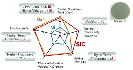
Figure 1. Features of GAN and SiC Mosfets compared to Si Mosfets [14].
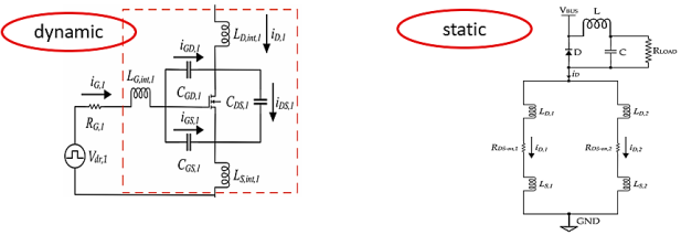
Figure 2. Factors affecting the process of controlling the performance of the switching process and balancing currents between transistors - Static and Dynamic States. [6].
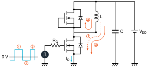
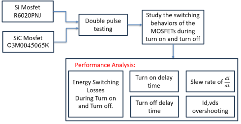
Figure 4. Block diagram of double pulse Testing.
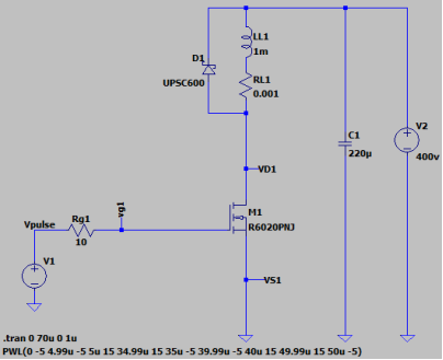
Figure 5. Electrical diagram of the double pulse test circuit on the R6020PNJ silicon transistor.
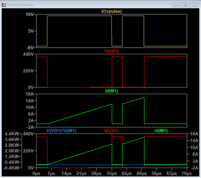
Figure 6. Driving pulses and voltage, current and power curves for the R6020PNJ silicon transistor.
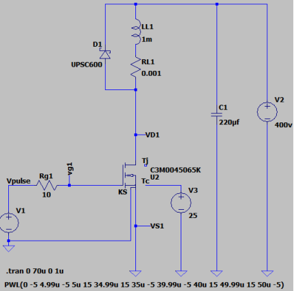
Figure 7. Electrical diagram of the dual pulse test circuit on a silicon carbide transistor C3M0045065K.
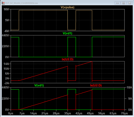
Figure 8. Driving pulses and voltage, current, and power curves for the C3M0045065K silicon carbide transistor.
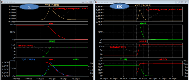
Figure 9. Voltage, current and power loss curves of the two transistors during Turn on operation.
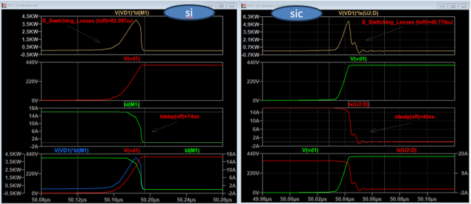
Figure 10. Voltage, current and power loss curves of the two transistors during Turn off operation.
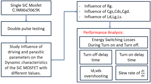
Figure 11. Block diagram of performance analysis of the effect of parasitic elements on the Dynamic characteristics of the silicon carbide transistors.
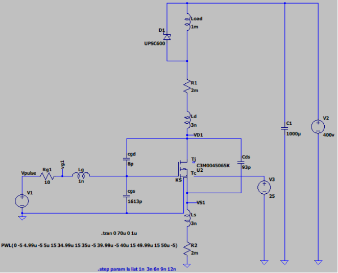
Figure 12. Double pulse Testing for Sic Mosfet under different Values of parasitic Components.
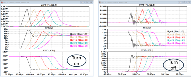
Figure 13. Voltage, current and power loss curves of the transistor during switching (on/off) operation for different Rg values.
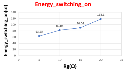
Figure 14. Energy Switching Losses during Turn on for Different Rg Values.
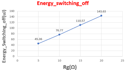
Figure 15. Energy Switching Losses during Turn off for Different Rg Values.
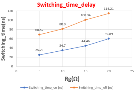
Figure 16. Switching Time Delay during Turn on/off for Different Rg Values.
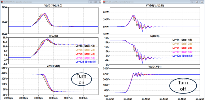
Figure 17. Voltage, current and power loss curves of the transistor during switching (on/off) operation for different Ls values.
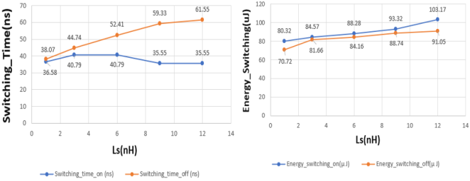
Figure 18. Switching Time Delay and Energy Loses during Turn on/off for Different Ls Values.
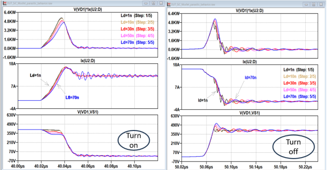
Figure 19. Voltage, current and power loss curves of the transistor during switching (on/off) operation for different Ld values.
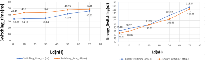
Figure 20. Switching Time Delay and Energy Loses during Turn on/off for Different Ld Values.
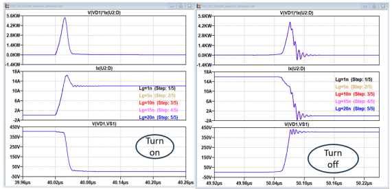
Figure 21. Voltage, current and power loss curves of the transistor during switching (on/off) operation for different Lg values.
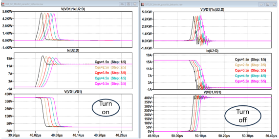
Figure 22. Voltage, current and power loss curves of the transistor during switching (on/off) operation for different Cgs values.
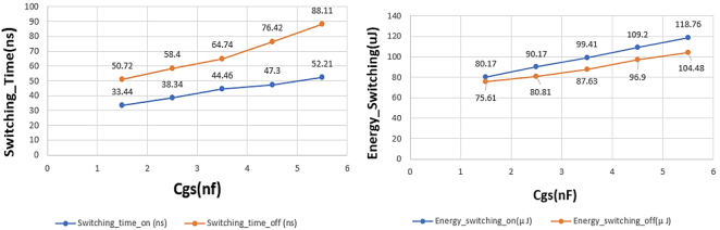
Figure 23. Switching Time Delay and Energy Loses during Turn on/off for Different Cgs.
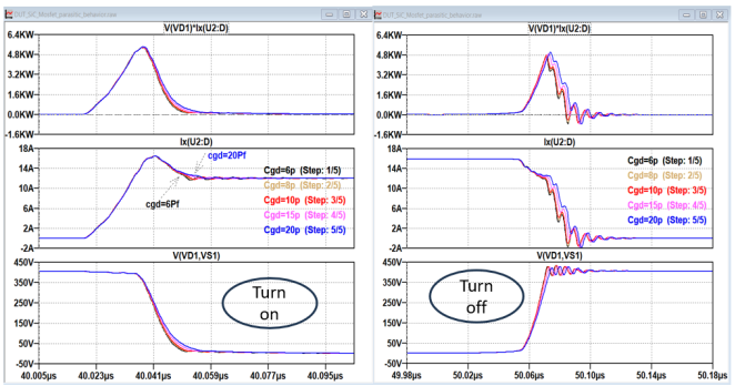
Figure 24. Voltage, current and power loss curves of the transistor during switching (on/off) operation for different Cgd values.
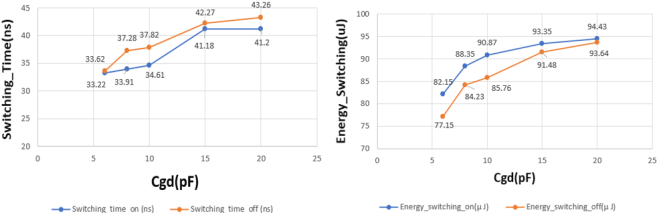
Figure 25. Switching Time Delay and Energy Loses during Turn on/off for Different Cgd.
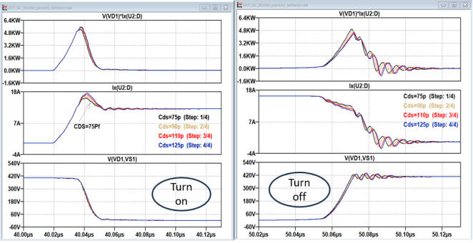
Figure 26. Switching Time Delay and Energy Loses during Turn on/off for Different Cds.
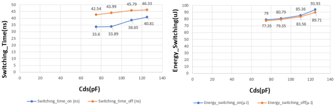
Figure 27. Switching Time Delay and Energy Loses during Turn on/off for Different Cds.
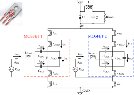
Figure 28. Parallel driving of silicon carbide Mosfets. [1].
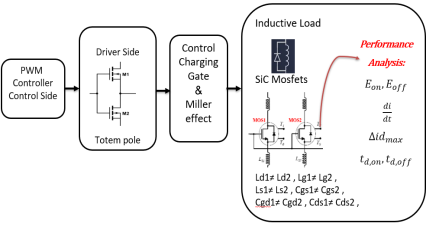
Figure 29. The block diagram of the parallel driving circuit.
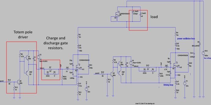
Figure 30. Circuit diagram for driving two C3M0045065K silicon carbide transistors in parallel.
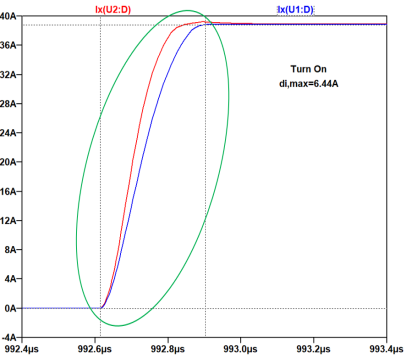
Figure 31. Simulation diagram of dynamic current imbalance at turn-on moment.
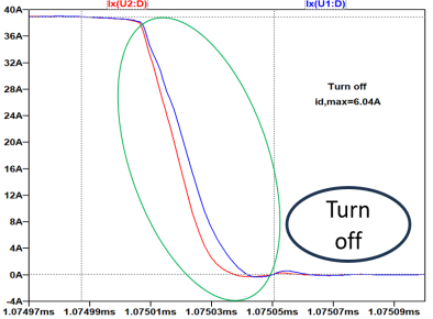
Figure 32. Simulation diagram of dynamic current imbalance at turn-off moment.
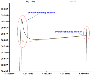
Figure 33. Simulation diagram of Overshooting dynamic current at turn-on/off moment.
Information